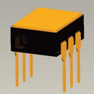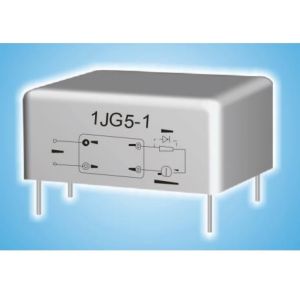
1JG3-1 DC Solid State Relay
Standard
Q/RY.J01111-2006
Application
Suitable for defense and industrial control fields, such as computer interfaces, digital circuit interfaces, signal transmission, numerical control equipment and measuring instruments. It is especially suitable for environments with harsh environments.
| Technical Parameters | Min. | Typ. | Max. | Unit | |
| Input Parameters | |||||
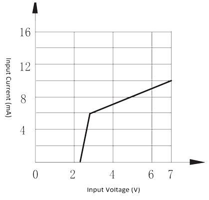
| Input voltage | (005) | 4 | 5 | 7 | Vd.c. |
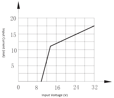
| (028) | 10 | 28 | 32 | Vd.c. | |
| Input current | (005) | 6 | 10 | mA | |
| (0028) | 12 | 20 | mA | ||
| Guaranteed turn-on voltage | (005) | 3.6 | Vd.c. | ||
| (0028) | 10 | ||||
| Guaranteed turn-off voltage | (005) | 1.5 | Vd.c. | ||
| (0028) | 3 | ||||
| Switch On time | 100 | μ s | |||
| Switch off time | 1000 | μ s | |||
| Reverse polarity | (005) | 7 | Vd.c. | ||
| (0028) | 32 | ||||
| Output parameters | |||||
| Number of output circuit groups | 1H (1 group N.O.) | ||||
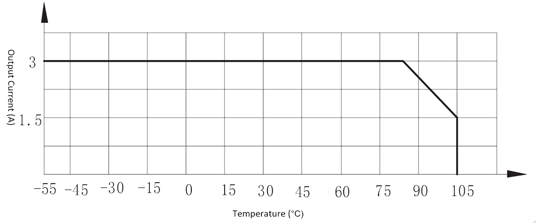
| Output current | 1×10⁻⁴ | 3.0 | A | ||
| Output voltage | 1 | 50 | Vd.c. | ||
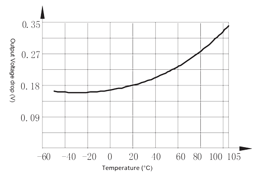
| Output voltage drop | 0.35 | Vd.c. | |||
| Output leakage current | 10 | μ A | |||
| Overload | 10.5 | A | |||
| Electrical insulation parameters | |||||
| Insulation resistance | 1000 | MΩ | |||
| Dielectric withstand voltage | 1000 | Vr.m.s. | |||
| Isolated capacity | 25 | pF | |||
| Environmental parameters | |||||
| Random vibration | 40 10~2000 |
(m/s2)2/Hz, Hz | |||
| Constant acceleration | 980 | m/s2 | |||
| Shock | 980, 6 | m/s2, ms | |||
| Storage temperature | -55~125 | ℃ | |||
| Operating temperature | -55~105 | ℃ | |||
| Other parameters | |||||
| Weight | 12 | g | |||
| Figure 1a. Input current vs. Input voltage (5 V) | Figure 1b. Input current vs. Input voltage (28 V) |
 |
 |
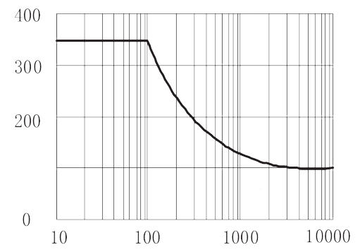
| Figure 2. Maximum output current vs. ambient temp. | |
 |
|
| Figure 3. Output voltage drop vs. temperature | Figure 4. Peak Surge Current vs. Surge Current Duration |
 |
 |
Mechanical drawings |
Bottom view Circuit |
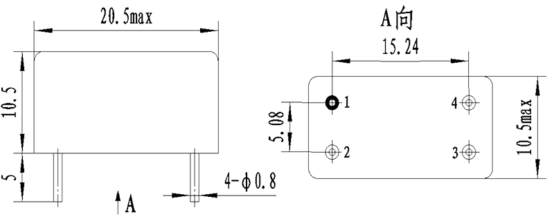 |
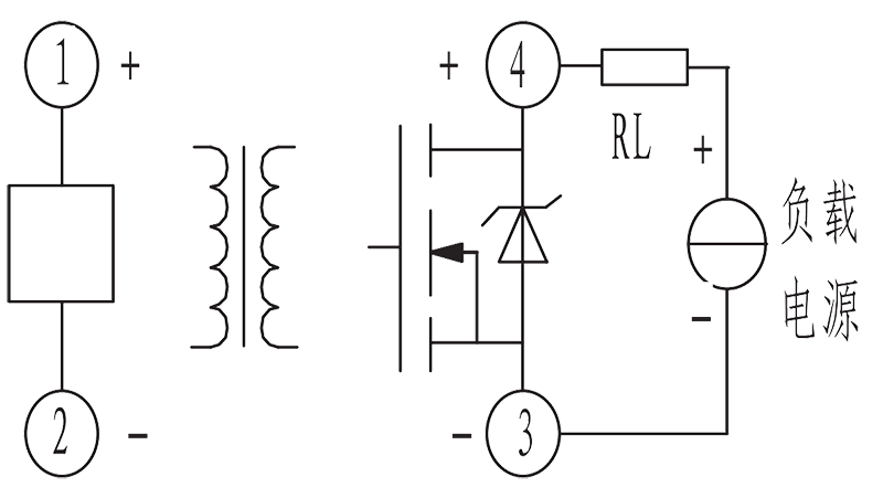 |
Order Mark
Example: 1JG3–1 005Y
| 1 | JG | 3 | – | 1 | 005 | Y |
| Number of outputs | Solid relay main name | Rated output current | Design Number | Specification No. (005: 5V, 028: 28V) | Screening level (Y or W) |