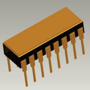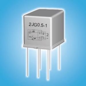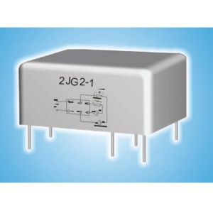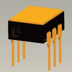
JGW-3015 MIL-Spec Photo-MOS Relay
Standard
Q/RY.J01159.1—2009
Application
Suitable for defense, scientific research, industrial control and modern management, such as isolated drive for aerospace, aviation and terrestrial electronic equipment, coupled amplification of digital signals, switching of analog signals, power transistor drive, measuring instruments, etc.
| Technical Parameters | Min. | Typ. | Max. | Unit | |||
Input |
|||||||
| Rated input current | 10 | mAd.c. | |||||
| Input current range | 5 | 20 | mAd.c. | ||||
| Input switching current | 5.0 | mAd.c. | |||||
| Input shutdown voltage | 0.8 | Vd.c. | |||||
| On time | 2.0 | ms | |||||
| Shutdown time | 0.5 | ms | |||||
Output |
|||||||
| Output configuration | Bidirectional | DC | |||||
| Number of output circuit groups | 1H (1 group N.O.) | ||||||
| Rated output current | ±2.5 | 4.5 | Ad.c. | ||||
| Rated output voltage | ±15 | 15 | Vd.c. | ||||
| Output leakage drop | ≤0.1 | ≤0.04 | Vd.c. | ||||
| Output leakage current | ≤1.0 | μA | |||||
| Transient voltage | ±20 | 20 | Vd.c | ||||
Electrical Insulation Specifications |
|||||||
| Insulation resistance | 1000 | MΩ | |||||
| Dielectric withstand voltage | 1000 | Vr.m.s. | |||||
| Power consumption | 0.79 | W | |||||
Environmental Specifications |
|||||||
| Seal leak rate | 5×10⁻³ | Pa·cm3/s | |||||
| Random vibration | 40 10~2000 |
(m/s2)2/Hz, Hz | |||||
| High Frequency Vibration | 294, 10~3000 | m/s2, Hz | |||||
| Constant acceleration | 49000 | m/s2 | |||||
| Shock | 14700, 0.5 | m/s2, ms | |||||
| Storage temperature | -55~125 | ℃ | |||||
| Operating temperature | -55~105 | ℃ | |||||
Other parameters |
|||||||
| Weight | 1.5 | g | |||||
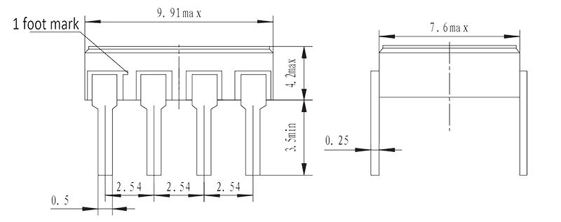
| Dimensions | 9.91×7.6×4.2 | mm | |||||
 |
 |
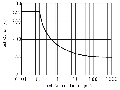 |
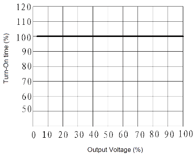
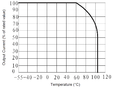
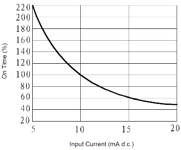
| Fig. 1: Turn-On time vs. Output Voltage | Fig. 2: Output Current vs. Temperature curve | Fig. 3: Inrush Current vs. Inrush Current duration curve |
 |
 |
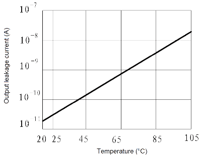 |
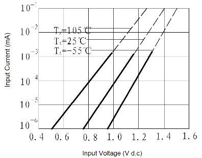
| Fig. 4: On time vs. Input Current curve | Fig. 5: Input Current vs. Input Voltage curve | Fig. 6: Output leakage current vs. Temperature curve |
Drawing |
|
 |
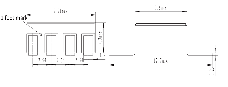 |
| DIP | SMD |
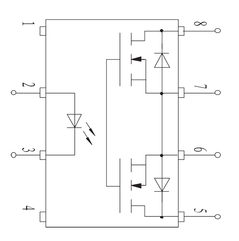
Internal circuit diagram |
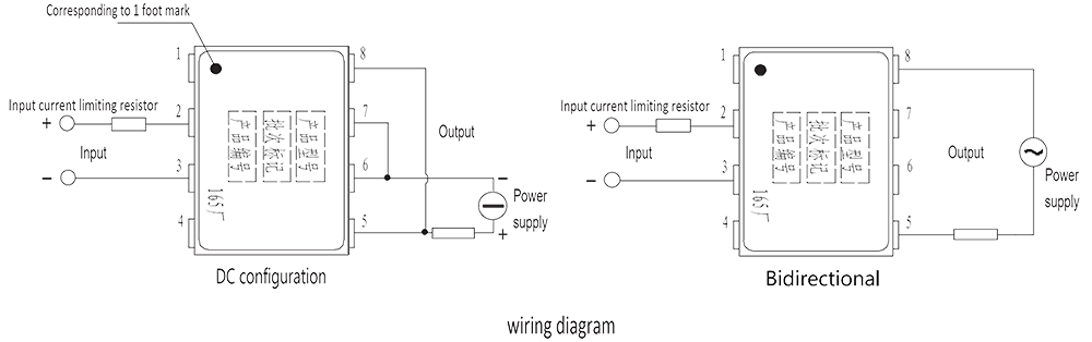
Overhead wiring diagram |
 |
 |
Order Mark
Example: JGW-3015 Y
| JG | W | – | 3015 | Y |
| Solid relay main name | Shape symbol (W, C or X) | Design Number | Screening level |
Note: The screening level (Y or W) and DIP/SMD should be indicated.