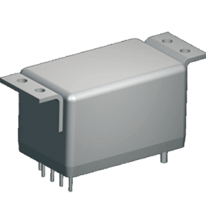
Characteristics
- Dual drive
- Input and output transformer isolation
- Low power
- All metal parallel seam sealing
- With status feedback function
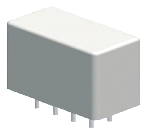
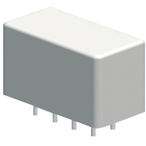
- Small size and light weight
- Fast response
Main Technical Characteristics
| Main Technical Parameters | Min | Typical | Max | Unit | ||
| Input | Input voltage | 4.5 | 5 | 5.5 | Vd.c. | |
| Control voltage | 5 | Vd.c. | ||||
| Power | 0.3 | W | ||||
| Control current | 6 | 10 | mA | |||
| Response time | 1 | μs | ||||
| Output | Output arrangement | 2H | ||||
| Output voltage | 9.5 | 11 | 13 | Vd.c. | ||
| Feedback voltage | ON | Low level | Vd.c. | |||
| OFF | High level | Vd.c. | ||||
| Other parameters | Insulation resistance | 100 | MΩ | |||
| Dielectric withstand voltage | 625 | Vpk(a.c.) | ||||
Environmental parameters
| Item | Min | Max | Unit |
| Operating temperature | -40 | 125 | °C |
| Storage temperature | -55 | 125 | °C |
| Shock | 500, 1 | (m/s2), ms | |
| Vibration (high frequency) | 30, 50~2000 | (m/s2)2, Hz | |
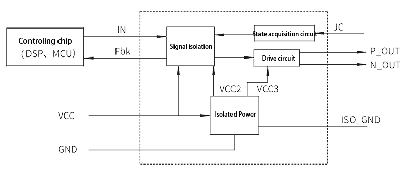
Circuit Diagram
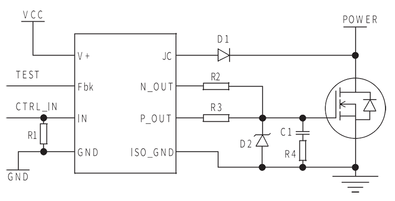 |
|
Take driving IRPF4368PBF as an example, the parameters of peripheral circuit components are selected as follows, turn-on time: 200μs, turn-off time: 100μ
Pin Description
| No. | Pin | Function | No. | Pin | Function |
| 1 | V+ | Power input “+” | 8 | N_OUT2 | 2nd way N channel output |
| 2 | Fbk1 | 1st way ON/OFF feedback output | 9 | P_OUT2 | 2nd way P channel output |
| 3 | IN1 | 1st way Drive control signal input | 10 | JC2 | 2nd way Detection signal output |
| 4 | ISO_GND1 | 1st way Isolated voltage output “-” | 11 | ISO_GND2 | 2nd way Isolated voltage output “-” |
| 5 | JC1 | 1st way Detection signal output | 12 | IN2 | 2nd way Drive control signal input |
| 6 | P_OUT1 | 1st way P channel output | 13 | Fbk2 | 2nd way ON/OFF feedback output |
| 7 | N_OUT1 | 1st way N channel output | 14 | GND | Power input “-” |
ON/OFF State Table
| Pin | IN | P_OUT | FBK | State description |
| 1 | L | L | H | MOSFET is not driven on |
| 2 | H | H | L | MOSFET drive on |
| 3 | L | L | L | Error (mistakenly ON) |
| 4 | H | H | H | Error (mistakenly OFF) |
| Dimensions (Unit: mm) | Working principle diagram and application instruction |
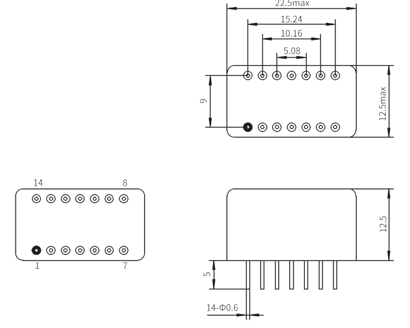 |
 |
Order mark
| DRV-3 | Y |
| Main code | Quality Grade |